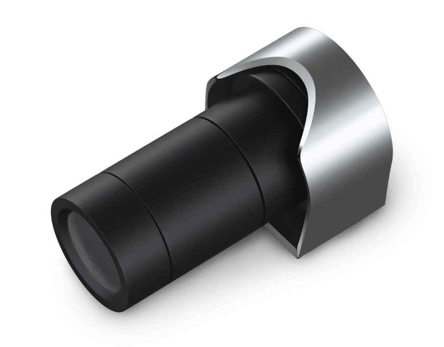
RProbe-2000 Overview
Module Features
- Precision: <0.01 nm or 0.01%
- Accuracy: <0.2% or 1 nm
- Stability: <0.02 nm or 0.03%
- Spot Size: Depends on objective (4 um to 200 um. 2mm)
- Sample Size: Platform dependent
Rtec Solution The RProbe-2000 provides real-time, one-click measurement and analysis of thickness, n&k, and roughness. This film thickness probe is easy to use with no expert knowledge required. Additionally, the system Includes a powerful analysis package scaling correction, multi-sample measurement, and dynamic measurement. Furthermore, with an extensive materials library (500+) and history of analysis: recall/display measurement results and statistics. Contact us to learn more about our film thickness measurement integration.
Need help or have a question?
Seamless Film Thickness Measurement Integration
RProbe-2000 film thickness probe across various solutions
Multi Function Tribometer, MFT-5000
Indentation and Scratch Tester, SMT-5000
3D Optical Profilometer, UP-5000
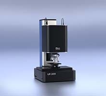
3D Universal Profilometer, UP-3000
Standard Configurations
The table shows the basic specification for the RProbe-2000.
| Model RProbe-2000-XX |
Wavelength Range | Spectrometer/Detector/Light source | Thickness Range* |
| Vsbl-a | 400-1100 nm | Spectrometer F4/Si 3600 pixels/ Tungsten – Halogen light source |
10 nm to 75 µm |
| UvVisbl | 200-1000 nm | Spectrometer F4/ Si CCD 2048 pixels/ Deuterium & Tungsten-Halogen light source |
1 nm to 75 µm (option: up to 150µm) |
| Vsbl | 700-1100 nm | HR Spectrometer F4/Si 2048 pixels/ Tungsten – Halogen light source |
1 µm to 400 µm |
| Nifr | 900-1700 nm | NIR F4/512 InGaAs PDA/Tungsten-Halogen light source | 50 nm – 100 µm |
| Vsbl-Nifr | 400-1700 nm | Spectrometer F4 Si CCD 3600 pixels(Vis channel);NIR F4/512 InGaAs PDA (NIR channel) Tungsten-Halogen light source |
10 nm – 100 µm |
| UvVsblNifr | 200-1700 nm | Spectrometer F4 Si CCD 2048 pixels (UVVis channel); NIR F4/512 InGaAs PDA( NIR channel) Deuterium & Tungsten-Halogen light source |
1 nm – 100 µm |
| Visbl-HF | 400-1100 nm | F4/Si 2048 pixels, Tungsten Halogen light source. High frequency measurement version of MProbe Vis system (LAN interface, 10µs integration time) |
10 nm – 70 µm |
| NifrHr | 1500-1550 nm | NIR F4/512 InGaAs PDA/Tungsten-Halogen light source or SLD (super-luminescent diode) | 10 nm – 1800 µm (quartz) 4 µm – 500 µm (Si) |
* T, n & k measurement in 25nm – 20µm thickness range. Maximum thickness limits are listed for R.I.= 1.5
Other configuration are available.
Film Thickness Probe Features
The RProbe provides reliable, traceable, and repeatable film thickness measurement and analysis.
Analysis of Translucent or Light absorbing films
This includes oxides, nitrides, photoresists, polymers, semiconductors, hard coatings, thin metal films, and many more
Thin Solar Cells
aSi, TCO, CIGS, CdS, CdTe – full solar stack measurement. LCD, FPD application: ITO, Cell Gaps, Polyamides.
Optical Coatings: dielectric filters, hardness coating, anti-reflection coating
Semiconductor and dialectics: Oxides, Nitrides, OLED stack
A Film Thickness Solution
The Film Thickness Probe is used extensively across a wide range of industries:
-
Aerospace
-
Hard Coating
-
Metal
-
Semiconductor
-
Polymer
Want to learn more?
Get in touch, and request a demo.
recommended
Information
© Copyright 2021 Rtec-Instruments - All Rights Reserved

