Halbleiter
Rtec Instruments bietet verschiedene Lösungen zur Bewertung von Touchscreens, elektronischen Komponenten, organischen Schichten, Beschichtungen, Leiterplatten, Konsumgütern und vielem mehr.
Unsere Lösungen
So viele Möglichkeiten. So viele Daten. Unsere Instrumente untersuchen und liefern umfassende Analysen für jede Phase der Halbleiterfertigung und Qualitätskontrolle.

Ritzhärte, Haftung, Härte
Mechanische Eigenschaften sind für die Halbleiterindustrie wichtig, da sie dabei helfen zu quantifizieren, ob eine Funktionsschicht auf den Substraten haftet oder ob die Eigenschaften zwischen verschiedenen Bereichen und Bauelementen variieren. Untersuchen Sie Kratzfestigkeit, Ritzhärte und Kratzbeständigkeit im Nano- und Mikrobereich. Ein integriertes 3D-Profilometer mit nm-Auflösung liefert 3D-Stitching-Bilder, um Beschichtungsfehler umfassend und eindeutig zu charakterisieren.
Reibung, Haltbarkeit, Verschleißbeständigkeit, Haptik, Grip
Charakterisieren Sie Reibung, Haltbarkeit und Verschleißmechanismen von Beschichtungen, Touchscreens, optischen Oberflächen, Konsumgütern und Linsen beschichtet mit verschiedenen mehrschichtigen Beschichtungen. Quantifizieren Sie Wahrnehmung, Haptik, statischen und dynamischen Reibungskoeffizienten unter vielfältigen Testparametern, Bewegungsformen und kontrollierten Umgebungsbedingungen.


Gekrümmte und flache Bildschirmoberflächen
Charakterisieren Sie Rauheit, Defekte, Kratzer und Merkmale mit unserer einzigartigen Optiktechnologie. Untersuchen Sie transparente, gekrümmte oder flache Bildschirme und Glasoberflächen mühelos. Untersuchen Sie außerdem die Haftung von Beschichtungen auf Oberflächen oder Geräten mit unserem Ritztester.
Pellikel (Fotolithographie)
Steigern Sie die Ausbeute und Prozesseffizienz, indem Sie das Abziehen und erneute Anbringen von Pellikeln vermeiden. Testen Sie die Position der Partikel auf dem Pellikel. Die einzigartige Technologie ermöglicht eine Quantifizierung und ermittelt, ob sich Partikel unterhalb oder oberhalb der Pellikeloberfläche befinden.


Chemisches Polieren
Untersuchen und charakterisieren Sie den CMP-Prozess wie nie zuvor. Zusätzlich zum Polieren von Wafern und Substraten verfügt der Tester über ein integriertes, optisches Oberflächenprofilometer.
3D-Bildgebung
Der einzigartige Alles-in-Allem-Universalprofiler vereint vier Bildgebungsmodi (konfokal, Interferometer, Dunkelfeld und Hellfeld) in einem Meßkopf. Dies ist für die Halbleiterindustrie von großem Vorteil, da die Vorzüge aller Techniken nahtlos miteinander kombiniert werden können. Zu den wenigen branchenüblichen Anwendungen gehören Partikel auf Pellikel, höchste XY-Auflösung auf Bauelementen und die Bildgebung transparenter Bildschirmoberflächen in einem Gerät.

Sehen Sie unsere Halbleiterprüfungen in Aktion
Sehen Sie sich an, wie unsere Instrumente all Ihre Anforderungen erfüllen können.
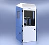
Sie benötigen Vielseitigkeit?
Sehen Sie sich das Multifunktions-Tribometer genauer an.
Suchen Sie Schwingungsverschleiß?
Sehen Sie sich unsere FFT-Schwingungsverschleißtester an.

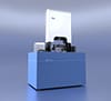
Benötigen Sie Härte- und Ritztests?
Erfahren Sie mehr über unseren Härte- und Ritztester SMT-5000.
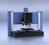
Benötigen Sie 3D-Mikroskopie?
Betrachten Sie unsere optischen 3D-Profilometer der UP-Serie.
Möchten Sie mehr erfahren?
Kontaktieren Sie uns und fordern Sie eine Demonstration an.
Leading innovation in surface and materials testing instrumentation.
recommended
Information
© Copyright 2021 Rtec-Instruments - All Rights Reserved