3D Optical Profilometer
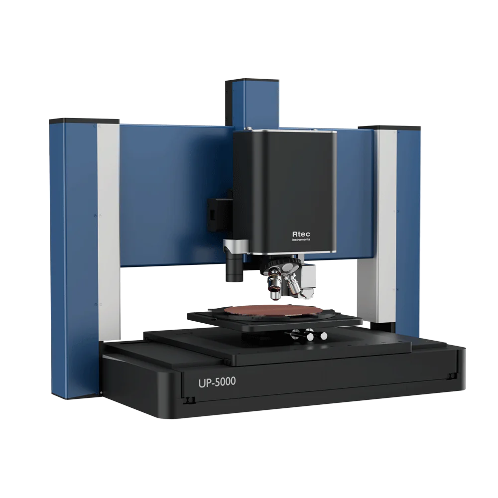
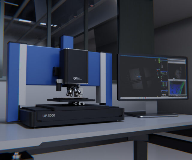
UP-5000 300 x 300 mm 3D Optical Profiler With AFM, Raman
A large-area 3D optical profilometer combining six imaging and analysis techniques — Confocal, White Light Interferometry, Spectral Film Thickness, Dark Field, Variable Focus, AFM, and Raman — on a 300 × 300 mm motorized stage. As a result, it enables wafer-scale and large-component surface metrology on a single platform.
KEY FEATURES
Six-in-One Optical Imaging Platform
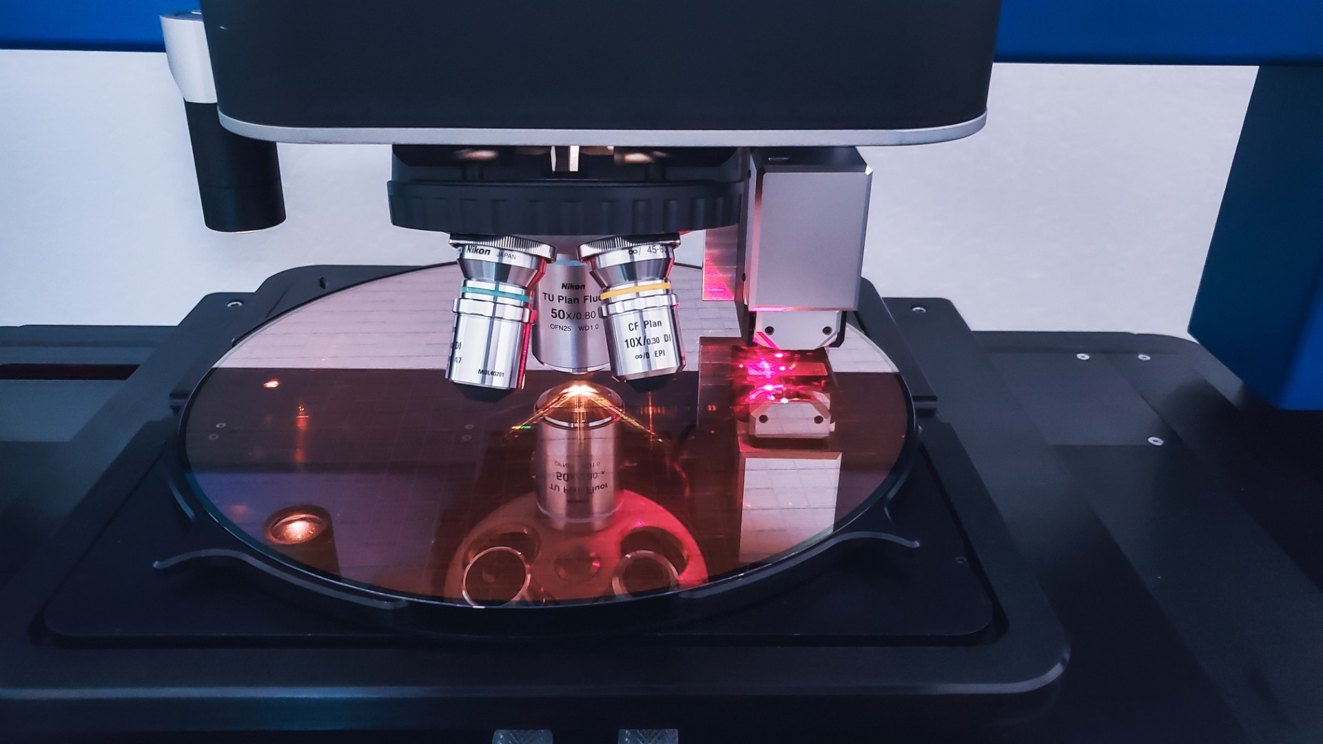
The UP-5000 integrates White Light Interferometry, Spinning Disk Confocal, Spectral Film Thickness, Dark Field, Variable Focus, and Bright Field modes. Furthermore, an AFM module and Raman spectroscopy are available as additional options, therefore bringing the total to eight measurement modalities on a single platform. Consequently, switching between modes requires no hardware changes or sample repositioning.
300 × 300 mm Stage for Large Sample Imaging
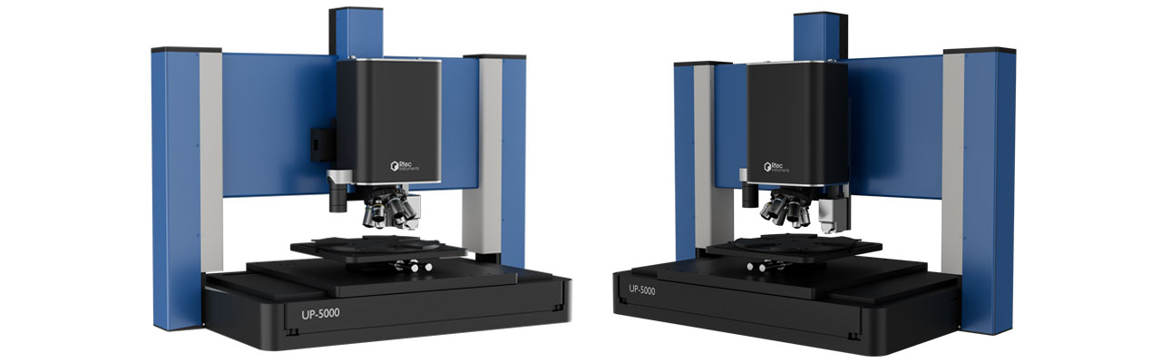
The UP-5000 is built around a 300 × 300 mm high-precision cross-roller XY stage. This therefore accommodates full semiconductor wafers, pellicles, large optical components, multi-sample fixture plates, and industrial test coupons that are too large for compact profilometers. Furthermore, precision encoding of the stage position supports seamless automatic stitching across the full sample area.
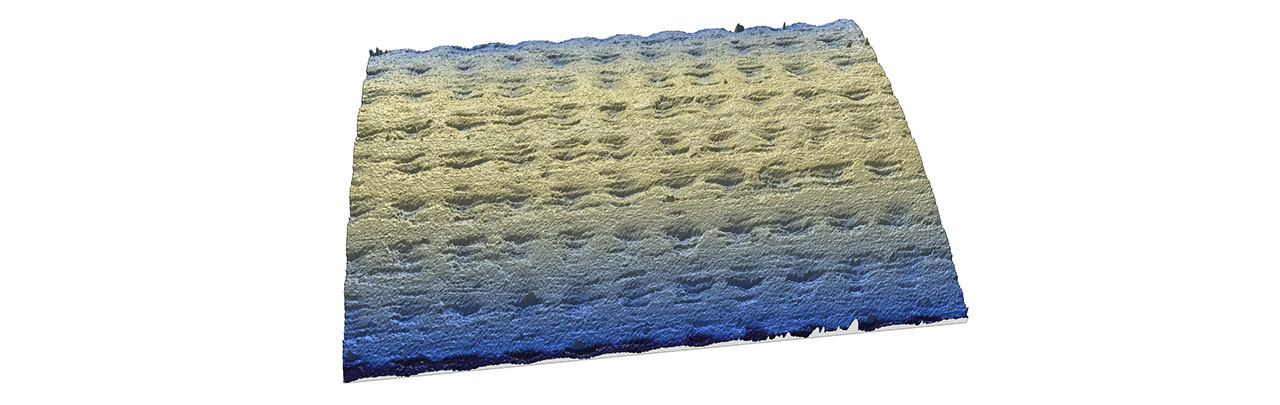
Best XYZ Resolution 3D Profilometer in Market
The UP-5000 Confocal technology provides the most accurate XY resolution among all optical techniques, even for areas with high slope. Furthermore, the integrated interferometry mode additionally gives the best Z resolution at any magnification.
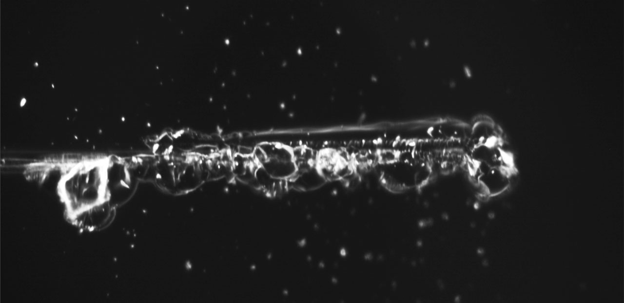
Dark Field Imaging
Microscope optics provides both bright field and dark field modes. Conventional systems, however, use bright field imaging only.
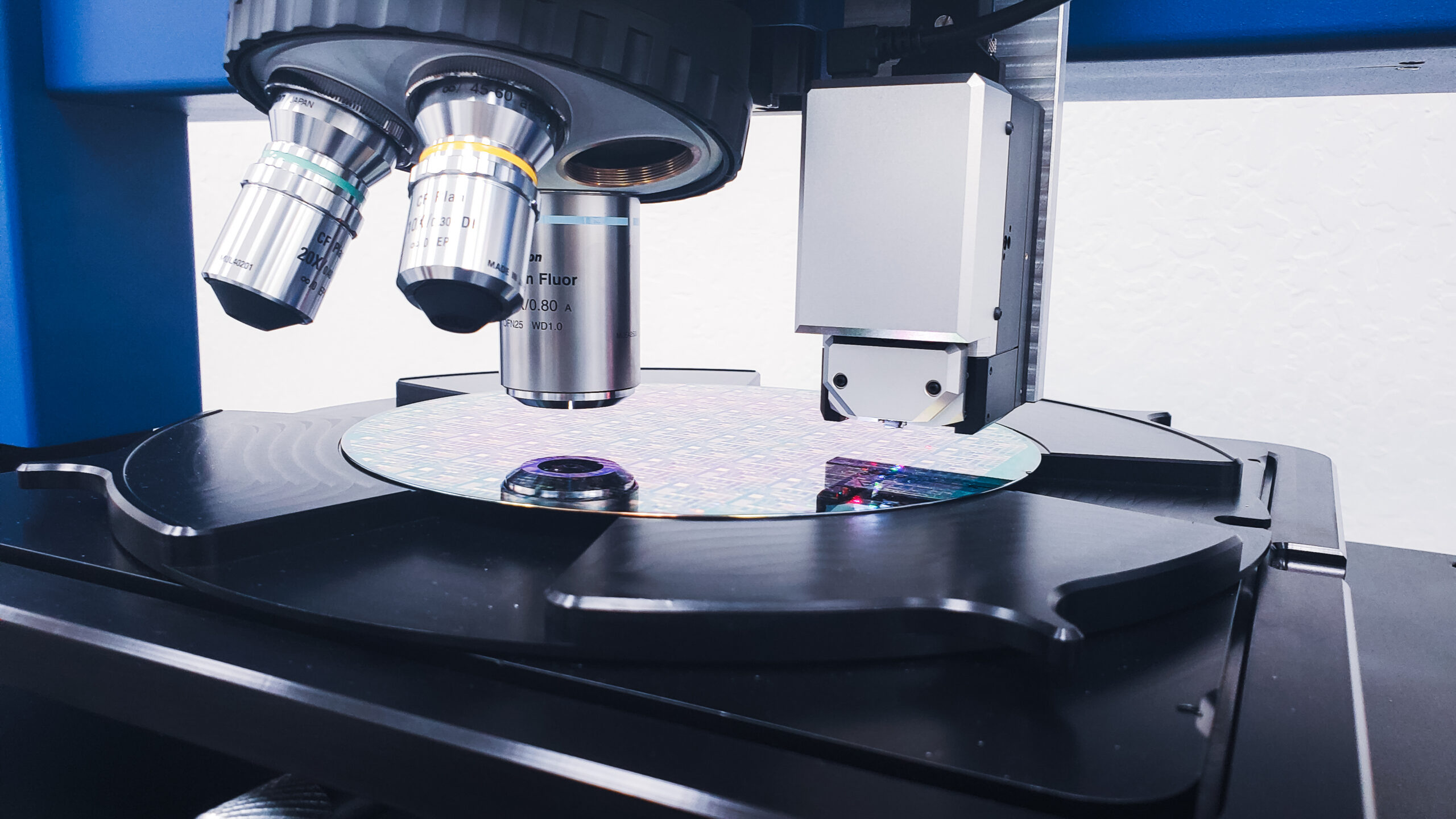
AFM, Raman, Film Thickness
Due to its open platform design and ample space, the UP-5000 allows mounting of several complementary techniques. As a result, the same test area can be analyzed comprehensively from multiple perspectives.
More about
Confocal – Spinning Disk
Fastest area scan – OR scan surface in an instant
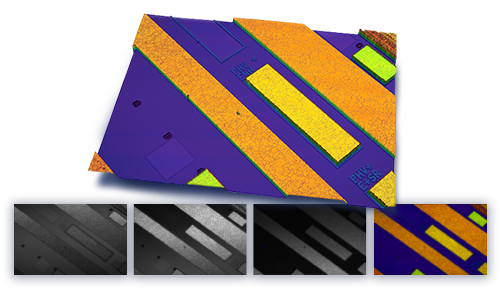
White Light Interferometry
Highest Z resolution in optical profilometry
Ultra Fast Film Thickness Determination
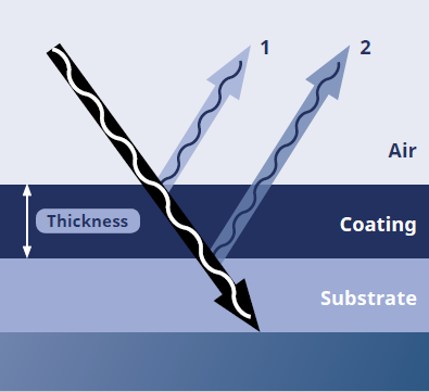
The film thickness measurement module uses spectral reflectance to measure the thickness of coated surfaces. No experience is necessary, as our one-click operation makes sample measurement straightforward. Furthermore, our extensive materials library of 500+ entries and multi-sample measurement capability provide comprehensive thickness analysis. As a result, non-contact high-accuracy step-heights and thickness values are delivered each time.
Atomic Force Microscope (AFM)
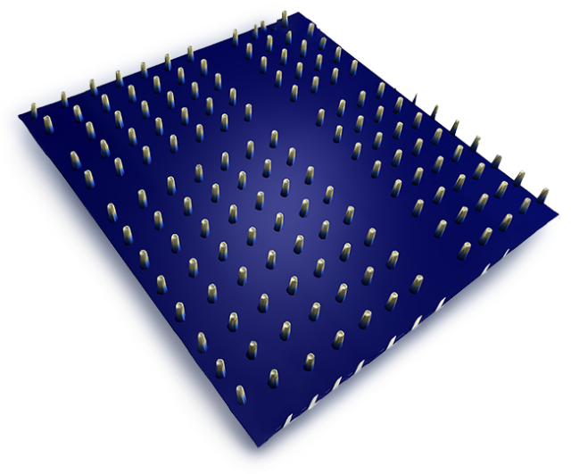
When surface features extend beyond the resolution limits of optical microscopy, the RTEC Atomic Force Microscope (AFM) delivers true nanometer-scale and atomic-level surface characterization. Using a precision scanning probe, the AFM generates ultra-high-resolution 3D images while measuring critical surface properties such as roughness, feature dimensions, defects, grain boundaries, phase contrast, and nanoscale morphology.
The system includes a comprehensive suite of measurement modes for topography, phase imaging, force measurements, and material property characterization, making it ideal for research and quality control in semiconductors, advanced materials, coatings, polymers, MEMS, and life sciences. Integrated with the RTEC Universal Profiler platform, users can seamlessly locate a region of interest using non-contact optical profilometry and, with a single click, acquire high-resolution AFM images of the exact same surface area. This correlated workflow combines the speed of optical metrology with the nanoscale precision of AFM, enabling comprehensive multi-scale surface characterization.
Variable Focus Imaging
Advanced focus stacking technology automatically combines images captured at multiple focal planes to create a perfectly focused, high-resolution image. The result is fast, non-contact visualization of complex 3D surfaces with outstanding detail, making inspection, defect analysis, and documentation easier and more reliabl
| Imaging Mode | Confocal, White Light Interferometry, Bright Field, Dark Field, and Variable Focus Imaging |
|---|---|
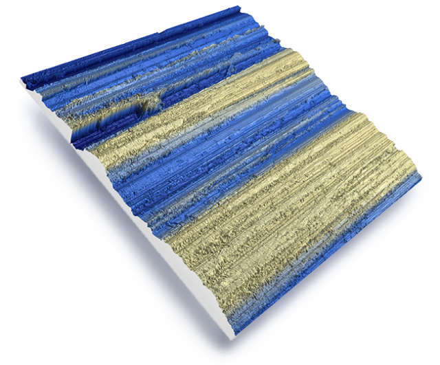
| Surface measurement | Roughness, 3D topography, step height, film thickness, defect analysis, crack inspection, and surface texture |
| Motorized XYZ stage | 300 × 300 × 150 mm |
| Standards | ISO 25178 - ISO 16610 - ISO 12781 - ISO 4287 - EUR 15178 |