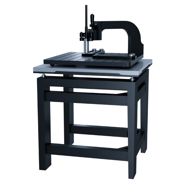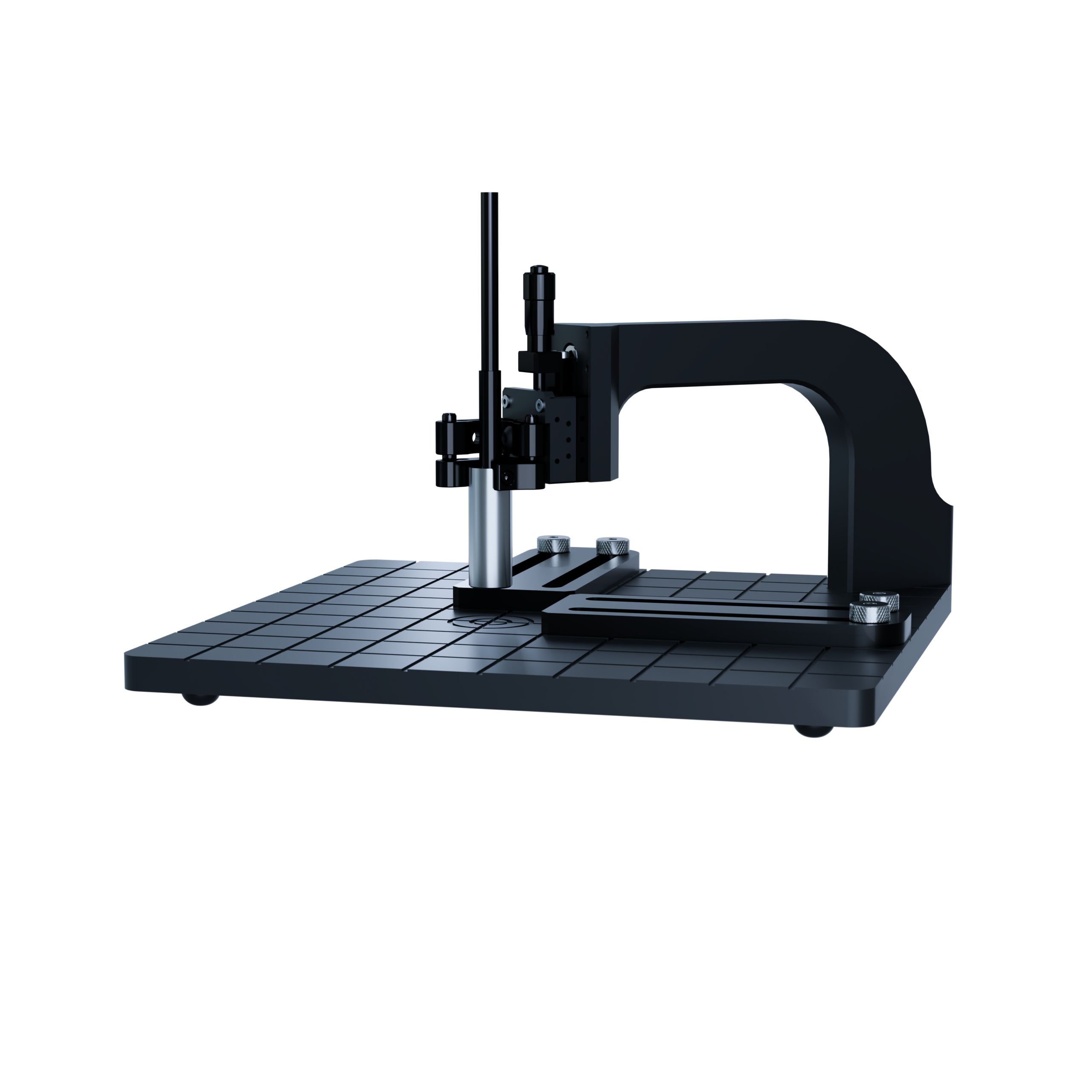
MFT-5000 Non-contact, non-destructive film thickness measurement with one-click operation.

MFT-5000マルチファンクショントライボメータは、高度な摩擦摩耗試験や表面分析用に設計された高精度システムです。さまざまな材料の摩擦、摩耗、潤滑性能、表面挙動の正確な測定が可能です。

このシステムは、コーティング、潤滑剤、燃料、金属、セラミック、ポリマー、ダイヤモンドのような超硬材料の試験をサポートしています。さらに、モジュラー設計と統合された測定技術により、ユーザーは実際の運転条件を単一のプラットフォームでシミュレートすることができます。その結果、研究用途と産業開発の両方をサポートします。

主な特長

UV, Visible, and NIR Configurations

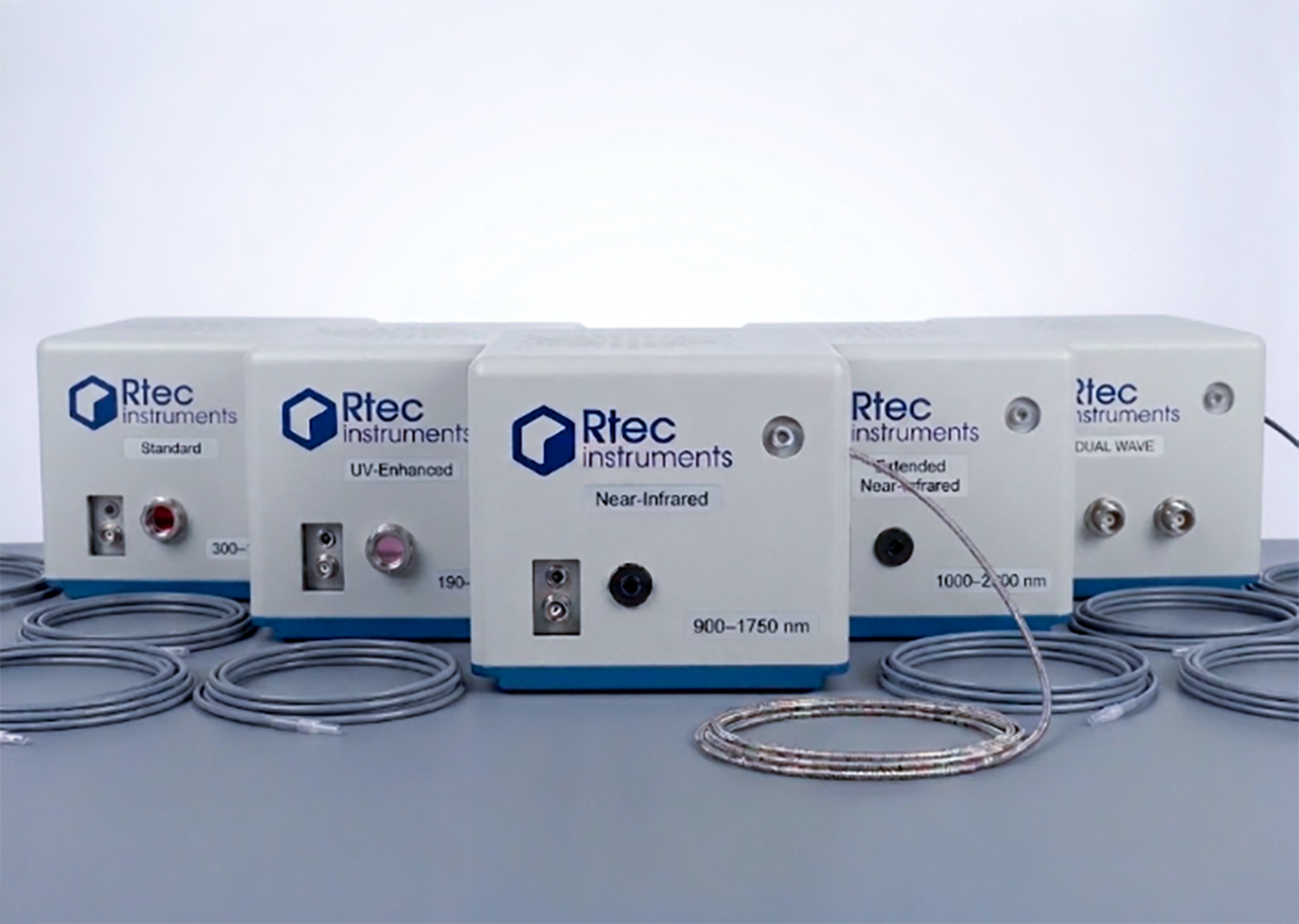
The TFT-1000 is offered in 300–1100 nm (Standard) 190–1100 nm (UV-Enhanced) 900–1750 nm (Near-Infrared) 1000–2500 nm (Extended Near-Infrared). Custom wavelength configurations available. Coating thickness dictates final choices.

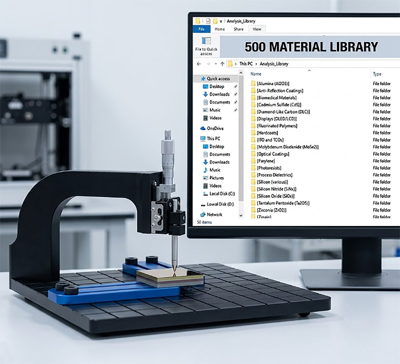
Library with over 500 materials included with every system

The 500+ materials library includes oxides, nitrides, photoresists, polymers, semiconductors, hard coatings, thin metal films, solar cell stack materials (aSi, TCO, CIGS, CdS, CdTe), LCD and display films (ITO, cell gaps, polyamides), optical coatings (dielectric filters, anti-reflection, hard coatings), and OLED stacks. Dynamic measurement mode acquires spectral data continuously while the sample is in motion, enabling coating uniformity maps across large substrates.

Spot Size down to few µm

The spot size depends on the objective lens used and ranges from 4 µm with high-magnification objectives to 200 µm–2 mm in low-magnification configurations. Small spots resolve patterned substrates and fine features; large spots average across a wider area for uniformity measurement.

High Precision and Stability

With stable and latest generation light sources and spectrometers, the TFT-1000 delivers precision suitable for thin film process control, coating quality verification, and in-line deposition monitoring.

Easy to Use with Latest-Generation Analysis Software

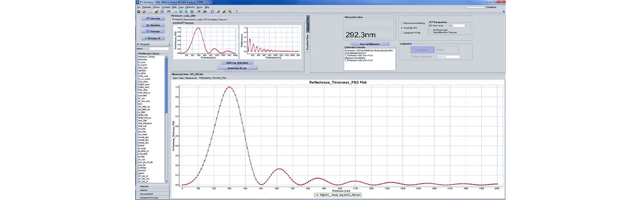
Every TFT-1000 ships with the full analysis package: one-click measurement, real-time spectral fitting, multi-layer optical modeling, and automated reporting. Thickness, refractive index, reflectance, and transmittance are extracted from a single acquisition — no software tiers, no add-on licenses. User can run the tool with under 5 minutes of training of software.

詳細はこちら

3D surface topography of tribological wear track showing material removal and wear depth – Rtec Instruments profilometer

Applications

Measure thickness, refractive index, reflectance, and transmittance of:

  • Single or multiple-layers
  • Transparent, translucent or lightly-absorbing films
  • Semiconductor- photo resist, dielectrics etc.
  • Optical Coatings
  • AR/VR devices
  • Medical – parylene, devices, cathetors

How does spectral reflectance film thickness measurement work?


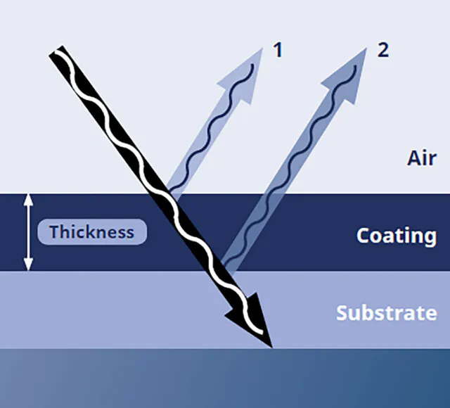
The probe shines white light onto the coated surface. Light reflects from both the top surface of the coating and the interface between the coating and the substrate. These two reflected beams interfere with each other, creating a wavelength-dependent pattern in the reflected spectrum. The spacing of the interference fringes encodes the optical thickness (n × d) of the film. With a known or fitted refractive index, the physical thickness d is calculated. This process happens in real time with one-click operation.

3D profilometry wafer surface profile showing micropillar array with sub-nanometer height measurement – Rtec Instruments UP-5000 optical profilometer

Wavelength300–1100 nm (Standard) 190–1100 nm (UV-Enhanced) 900–1750 nm (Near-Infrared) 1000–2500 nm (Extended Near-Infrared). Custom wavelength configurations available
Precisionnm range
Material Library500+

よくある質問

A thin film thickness tester is a non-contact optical instrument that measures coating thickness by analyzing light reflected from a coated surface. A spectral reflectance film thickness probe like the TFT-1000 extracts thickness, refractive index, reflectance, and transmittance from the interference pattern between light reflected at the film surface and at the film-substrate interface. Measurement takes seconds and requires no sample preparation.
The TFT-1000 measures film thickness from 1 nm to 1800 µm, plus refractive index, reflectance, and transmittance. It handles single layers and multi-layer stacks on transparent, translucent, and lightly absorbing films — photoresists, dielectrics, optical coatings, ITO, parylene, and solar or OLED stack materials among the 500+ in its library.
Semiconductor process engineers, optical coating manufacturers, display and AR/VR developers, solar cell producers, and medical device makers use the TFT-1000 for film thickness measurement in QC and R&D. Its non-contact operation and one-click workflow make it practical for both in-line production monitoring and laboratory analysis.
Yes. The TFT-1000 can be configured to measure multi-layer film stacks by fitting the measured reflectance spectrum to a multi-layer optical model. This is used for solar cell stacks, OLED layers, and complex optical coatings where multiple layers must be characterized simultaneously.
The minimum measurable thickness depends on the model configuration. The UV-visible model (200–1000 nm wavelength range) measures films as thin as 1 nm. The visible-range model measures from 10 nm, which is sufficient for most hard coatings, optical films, and semiconductor dielectrics. For ultra-thin gate oxides and monolayer films, the UV-visible model is appropriate.
No. The TFT-1000 is a non-contact probe that measures the as-received sample surface without cleaning, etching, or patterning. The only requirement is that the coating and substrate have sufficient optical contrast for the spectral reflectance measurement, which is the case for the vast majority of coating-substrate combinations.
The spot size depends on the objective lens used and ranges from 4 µm (high-magnification objectives) to 200 µm to 2 mm (low-magnification configurations). Smaller spot sizes are used for patterned substrates and small features; larger spots provide averaging over a wider area for uniformity measurements.
Yes. In addition to film thickness, the TFT-1000 measures refractive index, reflectance, and transmittance from the same spectral reflectance acquisition.
Measurement is real-time with one-click operation. The spectral acquisition and model fitting complete in seconds, and dynamic mode measures continuously while the sample moves.
The included library covers 500+ materials: oxides, nitrides, photoresists, polymers, semiconductors, hard coatings, thin metal films, solar stack materials (aSi, TCO, CIGS, CdS, CdTe), display films (ITO, polyamides), optical coatings, and OLED stacks.
Yes. Transparent, translucent, and lightly absorbing films are the core application of spectral reflectance film thickness measurement, on substrates from silicon to glass to polymer.

Ready to take your tribology
research to the next level?

Rtec Instrumentsの最先端ソリューションをご覧ください。当社の技術が、お客様の業務をどのように支援できるかをご確認ください。

当社の専門家にお問い合わせください